Learn Why AFM is an Essential Tool for R&D of 2D Materials and Devices
Today’s AFMs reveal not just the morphology of 2D materials, but also sense local electrical, mechanical, and functional properties in more ways than ever before
(Free download, compliments of Asylum Research, the Technology Leader in Atomic Force Microscopy)
Learn about techniques to characterize:
Nanoscale morphology
Lattice structure
Electrical and functional response
Mechanical properties (storage and loss moduli)
See actual examples on materials including:
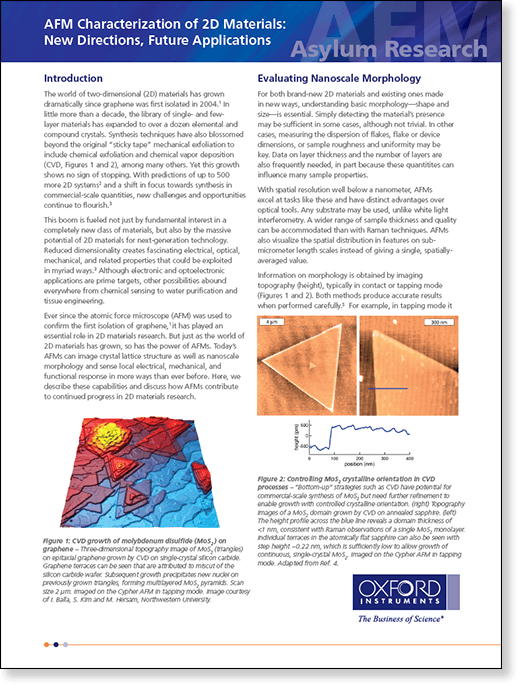
CVD growth of molybdenum disulfide (MoS2 )
Graphene exfoliation in ionic liquids
Lattice structure of a 2D optoelectronic material
Visualizing strain in epitaxial graphene grown on boron nitride (BN)
Mapping graphene grain orientation
Characterization of a photoswitchable MoS2 diode
Tuning band gap of a tungsten diselenide (WSe2 ) transistor<
 牛津仪器集团成员


 公安机关备案号31010402003473