原子力显微镜
AFM配件
应用
联系我们
 牛津仪器集团成员

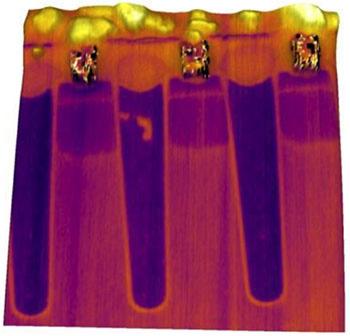
经过多年的发展,物理和电子设备的研究已扩展至化学、材料、机科学,以及工程学的所有分支,甚至是生物学。同时,在过去的20年里,原子力显微镜在多个科技进步领域发挥着重要的作用。Asylum Research生产的原子力显微镜为这些复杂的器件和材料提供了多种测量技术。就材料和器件的广度而言,目前市场上还缺乏能够与MFP-3D和Cypher原子力显微镜相媲美的仪器。
咨询AFM领域的专家• 测量局部电容和电阻、掺杂浓度(dC/dV)、损耗(dR/dV)的变化
根据功函数的差异、陷阱电荷或电压偏移,准确地测量表面接触电势
在快速力曲线的接触段中,在对样品施加偏压情况下测量电流
高水平的GUI代码为用户提供了自动化测量的灵活性,以优化研究时间
"Biodegradable electronic systems in 3D, heterogeneously integrated formats," J. K. Chang, H. P. Chang, Q. Guo, J. Koo, C. I. Wu, and J. A. Rogers, Adv. Mater. 30, 1704955 (2018). https://doi.org/10.1002/adma.201704955
"Local characterization of mobile charge carriers by two electrical modes: multi-harmonic EFM versus sMIM," L. Lei, R. Xu , S. Ye, X. Wang, K. Xu, S. Hussain, Y. J. Li, Y. Sugawara, L. Xie, W. Ji, and Z. Cheng, J. Phys. Commun. 2, 025013 (2018). https://doi.org/10.1088/2399-6528/aaa85f
"Multi-terminal memtransistors from polycrystalline monolayer molybdenum disulfide," V. K. Sangwan, H. S. Lee, H. Bergeron, I. Balla, M. E. Beck, K. S. Chen, and M. C. Hersam, 554, 500 (2018). https://doi.org/10.1038/25747
"Electrochemical strain microscopy probes morphology-induced variations in ion uptake and performance in organic electrochemical transistors," R. Giridharagopal, L. Q. Flagg, J. S. Harrison, M. E. Ziffer, J. Onorato, C. K. Luscombe, and D. S. Ginger, Nat. Mater. 16, 737 (2017). https://doi.org/10.1038/nmat4918
"Multifunctional logic demonstrated in a flexible multigate oxide‐based ‐double‐layer transistor on paper substrate," F. Shao, P. Feng, C. Wan, X. Wan, Y. Yang, Y. Shi, and Q. Wan, Adv. Electron. Mater. 3, 1600509 (2017). https://doi.org/10.1002/aelm.201600509
"Determining the resolution of scanning impedance microscopy using atomic-precision buried donor structures," D. A. Scrymgeour, A. Baca, K. Fishgrab, R. J. Simonson, M. Marshall, E. Bussmann, C. Y. Nakakura, M. Anderson, and S. Misra, Appl. Surf. Sci. 423, 1097 (2017). https://doi.org/10.1016/j.apsusc.2017.06.261
"Optically controlled electroresistance and electrically controlled photovoltage in ferroelectric tunnel junctions," W. J. Hu, Z. Wang, W. Yu, and T. Wu, Nat. Comm. 7, 10808 (2016). https://doi.org/10.1038/ncomms10808
"Analysis of conductance, read disturb and switching statistics in HfO2 RRAM using conductive ," A. Ranjan, N. Raghavan, J. Molina, S. J. O'Shea, K. Shubhakar, and K. L. Pey, Microelectron. Reliab. 64, 172 (2016). https://doi.org/10.1016/j.microrel.2016.07.112
" removal mechanism of copper chemical mechanical polishing in a periodate-based slurry," J. Cheng, T. Wang, Y. He, and X. Lu, Appl. Surf. Sci. 337, 130 (2015). https://doi.org/10.1016/j.apsusc.2015.02.076
"Carrier density modulation in a germanium heterostructure by ferroelectric switching," P. Ponath, K. Fredrickson, A. B. Posadas, Y. Ren, X. Wu, R. K. Vasudevan, M. B. Okatan, S. Jesse, T. Aoki, M. R. McCartney, D. J. Smith, S. V. Kalinin, K. Lai, and A. A. Demkov, Nat. Commun. 6, 6067 (2015). https://doi.org/10.1038/ncomms7067
"Two-dimensional quasi-freestanding molecular crystals for -performance organic - transistors," D. He, Y. Zhang, Q. Wu, R. Xu, H. Nan, J. Liu, J. Yao, Z. Wang, S. Yuan, Y. Li, Y. Shi, J. Wang, Z. Ni, L. He, F. Miao, F. Song, H. Xu, K. Watanabe, T. Taniguchi, J.-B. Xu, and X. Wang, Nat. Commun. 5, 5162 (2014). https://doi.org/10.1038/ncomms6162
"-mobility - transistors fabricated with macroscopic aligned semiconducting polymers," H.-R. Tseng, H. Phan, C. Luo, M. Wang, L. A. Perez, S. N. Patel, L. Ying, E. J. Kramer, T.-Q. Nguyen, G. C. Bazan, and A. J. Heeger, Adv. Mater. 26, 2993 (2014). https://doi.org/10.1002/adma.201305084
"Effective passivation of exfoliated black phosphorus transistors against ambient degradation," J. D. Wood, S. A. Wells, D. Jariwala, K.-S. Chen, E. Cho, V. K. Sangwan, X. Liu, L. J. Lauhon, T. J. Marks, and M. C. Hersam, Nano Lett. 14, 6964 (2014). https://doi.org/10.1021/nl5032293
"-voltage self-assembled monolayer - transistors on flexible substrates," T. Schmaltz, A. Y. Amin, A. Khassanov, T. Meyer-Friedrichsen, H.-G. Steinrück, A. Magerl, J. J. Segura, K. Voïtchovsky, F. Stellacci, and M. Halik, Adv. Mater. 25, 4511 (2013). https://doi.org/10.1002/adma.201301176
"Using nanoscale thermocapillary flows to create arrays of purely semiconducting single-walled carbon nanotubes," S. H. Jin, S. N. Dunham, J. Song, X. Xie, J. Kim, C. Lu, A. Islam, F. Du, J. Kim, J. Felts, Y. Li, F. Xiong, M. A. Wahab, M. Menon, E. Cho, K. L. Grosse, D. J. Lee, H. U. Chung, E. Pop, M. A. Alam, W. P. King, Y. Huang and J. A. Rogers, Nat. Nanotechnol. 8, 347 (2013). https://doi.org/10.1038/nnano.2013.56
"Ferroelectric---enhanced electroresistance in metal/ferroelectric/ tunnel junctions," Z. Wen, C. Li, D. Wu, A. Li, and N. Ming, Nat. Mater. 12, 617 (2013). https://doi.org/10.1038/nmat3649
"Strain-gated piezotronic transistors based on vertical zinc oxide nanowires," W. Han, Y. Zhou, Y. Zhang, C.-Y. Chen, L. Lin, X. Wang, S. Wang, and Z. L. Wang, ACS Nano 6, 3760 (2012). https://doi.org/10.1021/nn301277m
"Solid-state memories based on ferroelectric tunnel junctions," A. Chanthbouala, A. Crassous, V. Garcia, K. Bouzehouane, S. Fusil, X. Moya, J. Allibe, B. Dlubak, J. Grollier, S. Xavier, C. Deranlot, A. Moshar, R. Proksch, N. D. Mathur, M. Bibes, and A. Barthélémy, Nat. Nanotechnol. 7, 101 (2012). https://doi.org/10.1038/nnano.2011.213
"Single-layer MoS2 transistors," B. Radisavljevic, A. Radenovic, J. Brivio, V. Giacometti, and A. Kis, Nat. Nanotechnol. 6, 147 (2011). https://doi.org/10.1038/nnano.2010.279
"Creation of a two-dimensional electron gas at an oxide on silicon," J. W. Park, D. F. Bogorin, C. Cen, D. A. Felker, Y. Zhang, C. T. Nelson, C. W. Bark, C. M. Folkman, X. Q. Pan, M. S. Rzchowski, J. Levy, and C. B. Eom, Nat. Commun. 1, 94 (2010). https://doi.org/10.1038/ncomms1096
" resolution, sensitivity inorganic resists," J. Stowers and D. A. Keszler, Microelectron. Eng. 86, 730 (2009). https://doi.org/10.1016/j.mee.2008.11.034
"Tailoring GaN surfaces with biomolecules," E. Estephan, C. Larroque, F. J. G. Cuisinier, Z. Bálint, and C. Gergely, J. Phys. Chem. B 112, 8799 (2008). https://doi.org/10.1021/jp804112y
"Organic single-crystal - transistors of a soluble anthradithiophene," O. D. Jurchescu, S. Subramanian, R. J. Kline, S. D. Hudson, J. E. Anthony, T. N. Jackson, and D. J. Gundlach, Chem. Mater. 20, 6733 (2008). https://doi.org/10.1021/cm8021165
"Hunting the origins of line width roughness with chemical force microscopy," J. T. Woodward, J. Hwang, V. M. Prabhu, and K.-W. Choi, in CP931, Frontiers of Characterization and Metrology for Nanoelectronics (eds. D. G. Seiler, A. C. Diebold, R. McDonald, C. M. Gamer, D. Herr, R. P. Khosla, and E. M. Secula), AIP Conference Proceedings 931, 413 (2007). https://doi.org/10.1063/1.2799409
"Defect-free fabrication for single crystal silicon substrate by chemo-mechanical grinding," L. Zhou, H. Eda, J. Shimizu, S. Kamiya, H. Iwase, S. Kimura, and H. Sato, CIRP Ann. Manuf. Technol. 55, 313 (2006). https://doi.org/10.1016/S0007-8506(07)60424-7

© 牛津仪器 2026
 公安机关备案号31010402003473