原子力显微镜
AFM配件
应用
联系我们
 牛津仪器集团成员
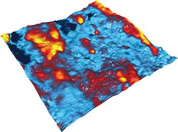
原子力显微镜特有的空间分辨率和直接探测能力使其成为纳米级电学性能表征的强大工具。Asylum Research生产的 MFP-3D™ 和 Cypher™ 系列可用于各种纳米级的电学性能表征。虽然“量化的电学测量”是这款的目标,但“电学模式”也经常用于快速检测、区分和识别样品中其他材料电学特性的性质差异。
Now with the Interferometric Displacement Sensor (IDS) Option for the Cypher AFM, d33 measurements using piezoresponse force microscopy are more reproducible and artifact-free. Interferometric detection directly measures cantilever deflection instead of cantilever angle that is utilized in conventional optical beam detection (OBD). IDS eliminates the artifacts due to electrostatic coupling. Download the data sheet in the white paper tab below.
咨询AFM领域的专家"Local characterization of mobile charge carriers by two electrical modes: multi-harmonic EFM versus sMIM," L. Lei, R. Xu, S. Ye, X. Wang, K. Xu, S. Hussain, Y. J. Li, Y. Sugawara, L. Xie, W. Ji, and Z. Cheng, J. Phys. Commun. 2, 025013 (2018). https://doi.org/10.1088/2399-6528/aaa85f
"Probing the ionic and electrochemical phenomena during resistive switching of NiO films," W. Lu, J. Xiao, L.-M. Wong, S. Wang, and K. Zeng, ACS Appl. Mater. Interfaces 10, 8092 (2018). https://doi.org/10.1021/acsami.7b16188
"Optimization of the Ag/PCBM interface by a rhodamine interlayer to enhance the efficiency and stability of perovskite solar cells," J. Ciro, S. Mesa, J. I. Uribe, M. A. Mejía-Escobar, D. Ramirez, J. F. Montoya, R. Betancur, H.-S. Yoo, N.-G. Park, and F. Jaramillo, Nanoscale 9, 9440 (2017). https://doi.org/10.1039/c7nr01678f
"Spatially resolved multicolor CsPbX3 heterojunctions via anion exchange," L. Dou, M. Lai, C. S. Kley, Y. Yang, C. G. Bischak, D. Zhang, S. W. Eaton, N. S. Ginsberg, and P. Yang, Proc. Natl. Acad. Sci. U.S.A. 114, 7216 (2017). https://doi.org/10.1073/.1703860114
"New insights on electro-optical response of poly(3,4-ethylenedioxythiophene):poly(styrenesulfonate) to humidity," E. S. Muckley, C. B. Jacobs, K. Vidal, J. P. Mahalik, R. Kumar, B. G. Sumpter, and I. N. Ivanov, ACS Appl. Mater. Interfaces 9, 15880 (2017). https://doi.org/10.1021/acsami.7b03128
"Mapping the photoresponse of CH3NH3PbI3 hybrid perovskite films at the nanoscale," Y. Kutes, Y. Zhou, J. L. Bosse, J. Steffes, N. P. Padture, and B. D. Huey, Nano Lett. 16, 3434 (2016). https://doi.org/10.1021/acs.nanolett.5b04157
"Grain boundary dominated ion migration in polycrystalline organic–inorganic halide perovskite films," Y. Shao, Y. Fang, T. Li, Q. Wang, Q. Dong, Y. Deng, Y. Yuan, H. Wei, M. Wang, A. Gruverman, J. Shield, and J. Huang, Energy Environ. Sci. 9, 1752 (2016). https://doi.org/10.1039/c6ee00413j
"‐performance and environmentally stable planar heterojunction perovskite solar cells based on a solution‐processed copper‐doped nickel oxide hole‐transporting layer," J. H. Kim, P.‐W. Liang, S. T. Williams, N. Cho, C.-C. Chueh, M. S. Glaz, D. S. Ginger, and A. K.‐Y. Jen, Adv. Mater. 27, 695 (2015). https://doi.org/10.1002/adma.201404189
"Gate-tunable memristive phenomena mediated by grain boundaries in single-layer MoS2," V. K. Sangwan, D. Jariwala, I. S. Kim, K. S. Chen, T. J. Marks, L. J. Lauhon, and M. C. Hersam, Nat. Nanotechnol. 10, 403 (2015). https://doi.org/10.1038/nnano.2015.56
"Polymer homo‐tandem solar cells with best efficiency of 11.3%," H. Zhou, Y. Zhang, C. K. Mai, S. D. Collins, G. C. Bazan, T. Q. Nguyen, and A. J. Heeger, Adv. Mater. 27, 1767 (2015). https://doi.org/10.1002/adma.201404220
"Observation and alteration of states of hematite photoelectrodes," C. Du, M. Zhang, J.-W. Jang, Y. Liu, G.-Y. Liu, and D. Wang, J. Phys. Chem. C 118, 17054 (2014). https://doi.org/10.1021/jp5006346
"Solvent‐polarity‐induced active layer morphology control in crystalline diketopyrrolopyrrole‐based band gap polymer photovoltaics," S. Ferdous, F. Liu, D. Wang, and T.P. Russell, Adv. Energy Mater. 4, 1300834 (2014). https://doi.org/10.1002/aenm.201300834
"Quantifying charge carrier concentration in ZnO films by scanning Kelvin microscopy," C. Maragliano, S. Lilliu, M. S. Dahlem, M. Chiesa, T. Souier, and M. Stefancich, Sci. Rep. 4, 4203 (2014). https://doi.org/10.1038/srep04203
"A new quantitative experimental approach to investigate single cell adhesion on multifunctional substrates," C. Canale, A. Petrelli, M. Salerno, A. Diaspro, and S. Dante, Biosens. Bioelectron. 48, 172 (2013). http://doi.org/10.1016/j.bios.2013.04.015
"Kelvin microscopy and electronic measurements in reduced oxide chemical sensors," C. E. Kehayias, S. MacNaughton, S. Sonkusale, and C. Staii, 24, 245502 (2013). https://doi.org/10.1088/0957-4484/24/24/245502
" spatial resolution Kelvin force microscopy with coaxial probes," K. A. Brown, K. J. Satzinger, and R. M. Westervelt, 23, 115703 (2012). https://doi.org/10.1088/0957-4484/23/11/115703
"Sub-30 nm scaling and -speed operation of fully-confined access-devices for 3D crosspoint memory based on mixed-ionic-electronic-conduction (MIEC) materials," K. Virwani, G.W. Burr, R.S. Shenoy, C.T. Rettner, A. Padilla, T. Topuria, P.M. Rice, G. Ho, R.S. King, K. Nguyen, A.N. Bowers, M. Jurich, M. BrightSky, E.A. Joseph, A.J. Kellock, N. Arellano, B.N. Kurdi, and K. Gopalakrishnan Kumar, in IEEE International Electron Devices Meeting 2012 Technical Digest (10-13 December 2012, San Francisco, CA), pp. 2.7.1-2.7.4. https://doi.org/10.1109/iedm.2012.6478967
"Photoinduced degradation studies of organic solar cell materials using Kelvin force and conductive scanning force microscopy," E. Sengupta, A. L. Domanski, S. A. Weber, M. B. Untch, H. J. Butt, T. Sauermann, H. J. Egelhaaf, and R. Berger, J. Phys. Chem. C 115, 19994 (2011). https://doi.org/10.1021/jp2048713
"Kelvin force microscopy studies of work function of transparent conducting ZnO:Al electrodes synthesized under varying oxygen pressures," R. Jaramillo and S. Ramanathan, Sol. Energy Mater. Sol. Cells 95, 602 (2011). https://doi.org/10.1016/j.solmat.2010.09.025
"Nanoscale, electrified liquid jets for -resolution printing of charge," J.-U. Park, S. Lee, S. Unarunotai, Y. Sun, S. Dunham, T. Song, P. M. Ferreira, A. G. Alleyene, U. Paik, and J. A. Rogers, Nano Lett. 10, 584 (2010). https://doi.org/10.1021/nl903495f
"Highly efficient solar cell polymers developed via fine-tuning of structural and electronic properties," Y. Liang, D. Feng, Y. Wu, S.-T. Tsai, G. Li, C. Ray, and L. Yu, J. Am. Chem. Soc. 131, 7792 (2009). https://doi.org/10.1021/ja901545q
"Differential conductivity in self-assembled nanodomains of a diblock copolymer using polystyrene-block-poly(ferrocenylethylmethylsilane)," J. K. Li, S. Zou, D. A. Rider, I. Manners, and G. C. Walker, Adv. Mater. 20, 1989 (2008). https://doi.org/10.1002/adma.200702796
"Space charge limited current measurements on conjugated polymer films using conductive atomic force microscopy," O. G. Reid, K. Munechika, and D. S. Ginger, Nano Lett. 8, 1602 (2008). https://doi.org/10.1021/nl080155l
"Near-static dielectric polarization of individual carbon nanotubes," W. Lu, D. Wang, and L. Chen, Nano Lett. 7, 2729 (2007). https://doi.org/ 10.1021/nl071208m
"Piezoelectric and semiconducting coupled power generating process of a single ZnO belt/wire. A technology for harvesting electricity from the environment," J. Song, J. Zhou, and Z. L. Wang, Nano Lett. 6, 1656 (2006). https://doi.org/10.1021/nl060820v
© 牛津仪器 2024
 公安机关备案号31010402003473